| ||||||||||||||||||||||||||||||||||||||||||||||||||||||||||||||||||||||||||||||||||||||||||||||||||||||||||||||||||||||||||||||||||||||||
Table of Contents | ||||||||||||||||||||||||||||||||||||||||||||||||||||||||||||||||||||||||||||||||||||||||||||||||||||||||||||||||||||||||||||||||||||||||
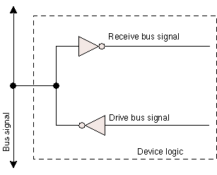
Communication between all system units in a PDP-11 configuration is done by a single common bus: the UNIBUS. All communication--both instructions and logical operations--is defined by a set of 56 signals. This set of 56 signals is used for program controlled data transfers, direct memory data transfers, priority bus control, and program interrupt. General Concepts of the UNIBUSThere are five major aspects of the UNIBUS that affect both software and hardware considerations in the PDP-11. Single BusThe set of 56 signals that comprise the UNIBUS is the one and only bus connecting all peripheral devices, memories, and the central processor. Thus, to every device there exists a single set of signals by which it can be interrogated by the processor or other devices, or be used by the device itself to transfer data to and from memory. The processor uses this same set of signals to communicate with all memories and devices. The important point here is that the form of the communication used by processor and peripheral devices is identical. Consequently, the same set of program instructions used to reference memory is used to reference peripheral devices. Peripheral devices in a PDP-11 system are designed to respond to the UNIBUS in the same manner as memory. Device status registers, device control registers, and device data registers are each assigned unique "memory" addresses. For example, the instruction Bidirectional BusUNIBUS bus signals are bidirectional--the signal received as an input can be driven as an output, as shown in the figure below.
Master-Slave RelationshipAt any one point in time, there is one device--called the master--that has control of the bus. The master device controls the bus to communicate with other devices--called slaves--on the bus. An example of this relationship is the processor (master) fetching an instruction from memory (which is always a slave). Interlocked CommunicationFor each control signal issued by the master device, there is a response from the slave; thus bus communication is independent of the physical bus length and the response time of the master and slave devices. Also, master-slave relationships can exist in nearly any combination between fast-responding and slow-responding devices. Dynamic Master-Slave RelationMaster-slave relationships are dynamic. The processor, for example, can pass bus control to a disk. The disk, as master, could then communicate with a slave memory bank. UNIBUS signalsThe 56 UNIBUS signals can be divided into two major groups--the interrupt group and the non-interrupt group. The interrupt group can then be subdivided into two classes--the request and control class and the grant class. All bus signals except the grand class are bidirectional in nature and are connected to every device (though they may not be used by every device). The grant signals, because of their special nature in priority bus control, are bussed through each device and are unidirectional in nature. Data Transfer SignalsData Lines (D<15:00>)Note that the notation The 16 data lines are used to transfer information between master and slave. This is the bit format:  Address Lines (A<17:00>)The 18 address lines are used by the master device to select the slave (a unique core memory or device register address) with which it will be communicating. This is the bit format of the 18 signals: 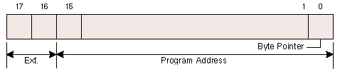
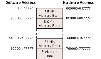
An address map is shown in below.
The peripheral bank is composed of the processor's fast memory, status register, console switch register, and all device registers. Control Lines(C<1:0>)These two bus signals are coded by the master device to indicate to the slave one of four possible data transfer operations. Master Synchronisation and Slave Synchronisation ( |
![[Home]](/images/dirHome.gif)


C1 | C0 | Transfer |
|---|---|---|
0 | 0 | DATI - Data In |
0 | 1 | DATIP - Data In, Pause |
1 | 0 | DATO - Data Out |
1 | 1 | DATOB - Data Out, Byte |
DATO and DATOB
The DATO and DATOB operations are used to transfer data out of the master to the slave.
DATO is used to transfer a word to the address specified by A<17:01>. The slave ignores A00 and the data appears on D<15:00>.
DATOB is used to transfer a byte of data to the address specified by A<17:00>. A00 = 0 indicates the low byte, and data appears on D<07:00>; A00 = 1 indicates the high byte, and data appears on D<15:08>.
DATI and DATIP
The DATI and DATIP operations transfer data from a slave whose address is specified on A<17:01> into the master. Both transfers are made in words on D<15:00>. In destructive read-out devices, DATI commands a read-write operation, while DATIP commands a read operation only and sets a pause flag.
When the device receives the subsequent DATO or DATOB and its pause flag is set, the usual read cycle is skipped and an immediate write cycle is initiated. Thus, DATIPs are immediately followed by DATO or DATOB to effect a read-modify-write data exchange.
In non-destructive read-out devices, DATI and DATIP are treated identically.
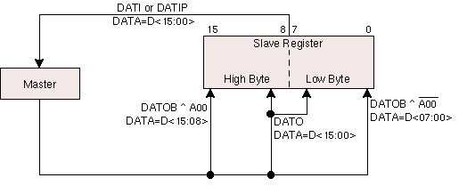
This diagram illustrates the data flow in the four data transfers:
 |
| Figure:Data Flow |
Note that all transfers into the master are word operations; it is up to the master to accept the appropriate byte. On a DATOB, the master must place the byte on the appropriate data lines; the slave must accept the proper byte.
Data Transfer Examples
The bus operations used by the processor for a typical instruction sequence illustrates how the data transfer operations are used. The "program" starts at location 1000:
|
where R0 contains 500 and location 500 contains 10023. The result of this instruction sequence will leave 10027 in location 500. In binary form, this coding appears as:
|
The following table lists the bus operations that result as a consequence of these two instructions:
| Processor Cycle | Bus Operation | Bus Address | Data Transferred |
|---|---|---|---|
| 1. Fetch | DATI | (PC) = 001000 | 105210 |
| 2. Destination | DATIP | (R0) = 000500 | 010023 |
| 3. Execute | DATOB | (R0) = 000500 | 000024 |
| 4. Fetch | DATI | (PC) = 001002 | 062710 |
| 5. Source | DATI | (PC) = 001004 | 000003 |
| 6. Destination | DATIP | (R0) = 000500 | 010024 |
| 7. Execute | DATO | (R0) = 000500 | 010027 |
Note that in step 3, it is inconsequential what appears on D<15:08>; the slave accepts only the modified low byte.
A second example of bus operation compares the contents of the teletype keyboard data buffer whose address is 177560 with the ASCII value for the letter "A."
|
This instruction is assembled in three words as follows:
|
The processor will execute this instruction with these cycles:
| Processor Cycle | Bus Operation | Bus Address | Data Transferred |
|---|---|---|---|
| 1. Fetch | DATI | (PC) = 200 | 123727 |
| 2. Source | DATI | (PC) = 202 | 177560 |
| 3. Source | DATI | 777560 | ASCII |
| 4. Destination | DATI | (PC) = 204 | 000301 |
| 5. Execute | None | None | Condition codes set internally. |
Note that in step 3, the software specified address 177560 was converted to the bus address 777560.
Signal Description of Data Transfers
The figure below shows the signal flow between master and slave during a DATO operation2. The master sets Control for DATO, sets Address for the unique slave address, and sets Data for the information to be transferred. The master then asserts MSYN.
This signal is received by the slave that recognises its address; it responds by accepting the data and asserting SSYN. SSYN is received by the master which then negates Control, Address, Data, and MSYN. The slave sees MSYN negated and negates SSYN.
The master device continues its operation when it sees SSYN negated.
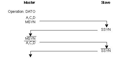 |
| Figure:DATO Flow |
The flow of signals for DATI is shown below.3
The master sets Control for DATI, sets Address for the slave to be selected, and then asserts MSYN.
The selected slave responds by setting Data for the information requested and assets SSYN.
The master sees SSYN, accepts the data, and then negates Control, Address, and MSYN. The slave sees MSYN negated and negates SSYN. The master continues when it sees SSYN negated.
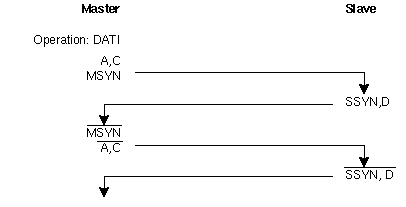 |
| Figure:DATI Flow |
UNIBUS Control Operations
The following section will deal with how a device becomes master of the bus and how control of the bus is transferred from one device to another. Two additional bus operations will be presented--the PTR (Priority Transfer) and INTR (Interrupt).
In normal operation, the processor is bus master, fetching instructions and operands from memory. Other devices on the bus have the capability of becoming bus master, and use the bus for one of two purposes:
- To gain direct memory access, or
- To interrupt program execution and force the processor to branch to a specific address.
Priority Arbitration
Transfer of bus control from one device to another is determined by a priority scheme in which three factors must be considered.
First, the processor's priority is determined by bits 7, 6, and 5 in the processor status register. These three bits set a priority level that inhibits granting of bus requests on lower levels.
Second, bus requests from external devices can be made on one of five request lines. NPR ha the highest priority, and its request is honored by the processor between bus cycles of an instruction execution. BR7 is the next highest; BR4 is the lowest. These four lower level requests are honored by the processor between instructions, except when the instruction currently being executed causes an internal trap (either an error or trap instruction).
In this case, BR requests will not be honored until completion of the first instruction after the trap sequence. Thus if two requests are made to the processor for bus control, the higher of the two requests will be honored first.
Third, in response to a bus request, the processor may honor the request by asserting a bus grant (BG) corresponding to the line on which the bus request was made. This signal is passed serially through each device in the system. If a device had made a request, it would block the grant signal and prevent it from reaching the following devices. Thus, in this "pass-the-pulse" chain, the device that is closest to the processor has the highest priority on that request level.
This table lists devices priorities:
| Priority | Devices |
|---|---|
| Highest | Devices on NPR |
| Processor when priority = 111 | |
Devices on BR7 | |
| Processor when priority = 110 | |
Devices on BR6 | |
| Processor when priority = 101 | |
Devices on BR5 | |
| Processor when priority = 100 | |
Devices on BR4 | |
| Processor when priority = 011 | |
| Internal options | |
| Processor when priority = 010 | |
| Internal options | |
| Processor when priority = 001 | |
| Lowest | Internal options |
| Processor when priority = 000 |
When the processor's priority is set at N, all requests for bus control at level N and below are ignored.
Selection of Next Bus Master
The signal sequence by which a device becomes selected as the next bus master is the PTR (Priority Transfer) bus operation. Note that this operation does not actually transfer bus control; it only selects a device as next bus master.
It takes one additional condition to complete the transfer: the current bus master must complete its bus operations.
The signal that indicates this is BBSY. Thus, when a device makes an NPR or BR request to the processor for bus control, it waits until it first becomes selected as next bus mater by the PTR operation and second, it no longer senses BBSY.
The negation of the the BBSY signal indicates that the current master has completed its bus operation. The selected device now becomes bus master and asserts BBSY itself.
Interrupt Sequence
Once the device has bus control and is asserting BBSY itself, it is sole user of the bus until it releases its control. This release of control can be made either actively or passively. Passive release is realised by negating BBSY. Bus control will then pass to either a device that was selected in the meantime by another PTR sequence or back to the processor, which will continue where it was interrupted. Active release of bus control is realised through the INTR bus sequence.
The INTR (Interrupt) operation is used by the bus master to transfer to the processor a memory address (called the interrupt vector). Two consecutive words, the starting address of an interrupt service routine and a new processor status word, are stored at the interrupt vector address. After the INTR operation is complete, the processor automatically becomes bus master and begins a trap sequence in which it stores the current value of the PC and PS on the stack and fetches a new PC and PS from the location pointed to by the interrupt vector. Thus, the next instruction executed is the start of the interrupt service routine.
It is illegal to issue an INTR command after gaining control of the bus by requesting on an NPR line. NPR requests are granted during instruction execution and external bus masters must restrict their bus use to non-processor activities.
Interrupt Servicing Sequence Example
The following is an example of the INTR sequence.
When a peripheral requires service and requests control of the bus with a BR signal, the operations undertaken to "service" the device are as follows:
- Gain control of the bus -- when the processor has no higher priority tasks to complete, it relinquishes the bus to that device. Higher priority items are (in order of priority):
- Acknowledging an
NPRrequest - Handling a processor error (illegal instructions, requirements for non-existent memory, etc.)
- Completing the current instruction
- Acknowledging a trace trap
- Continuing a higher priority process
- Acknowledging a higher level
BRsignal - Acknowledging same level
BRsignals for devices closer to the processor.
- Acknowledging an
- Do
INTRsequence -- when the device has control of the bus, it initiates anINTRsequence, transferring to the processor the interrupt vector address which specifies two words in memory containing the address and status of the appropriate device service routine. - Push old interrupt vector onto stack -- the processor then "pushes"--first, the current central processor status (
PS) and then the current program counter (PC) onto the processor stack. - Fetch new interrupt vector -- the new
PCandPS(the "interrupt vector) are taken from the address specified by the device, and the device service routine is begun. Note that those operations all occur automatically and that no device polling is required to determine which service routine to execute.
Example of an NPR operation
Disk operation gives an example of a device which uses the bus for direct memory access. Under program control, the processor would initialise registers in the disk control that specify word count (WC, number of words in a block of data to be transferred), memory address (MA, the address at which the block of data is found or loaded), and track address (TA, the point on the disk where the block of data starts).
Also, the program would set certain function bits in the disk's command and status register that specify a read or write function. For this example, assume the disk was set to read.
Once the disk's control registers are initialised, the disk control logic starts a search for the requested data. (The processor in the meantime has continued in its program execution.) When the disk has found the data, it assembles the first 16-bit word from the disk surface into its data register. The disk now requests bus control via the NPR request line. The processor, when it has completed its current bus cycle of the current instruction and no higher NPR requests exist, grants control of the bus to the disk. The disk, as bus master, effects a DATO bus operation, transferring the contents of its data buffer to the core address held in its MA. The MA is now incremented and the WC is decremented. When the DATO operation is complete, the disk passively releases control of the bus.
When the second word has been assembled, the disk again requests bus control, does a data transfer, and then releases bus control. This cycle is repeated until the WC reaches zero. At this point, the disk has completed the transfer that was requested.
To notify the program that the transfer is finished, the disk initiates a request for bus control at the BR level, gains control when higher priority requests are satisfied, and does an immediate INTR to the processor and causes the program to branch to a specific service program (as described in the previous example).
| Return to top | |
| Created: |
|---|